Geek My Ride: Learning to speak OBD-II

Cars are pretty interesting, but generally not especially so from a Digital Electronics geek’s perspective. GPS navigation systems and fuel-consumption computers are cool, but for the most part, cars seem to be solidly the bailiwick of Mechanical types.

Relatively new cars, though, have a hidden secret. Every new car sold in the US since 1996 is required to implement OBD-II — a collection of protocols for the interchange of information about various automotive parameters. Information such as engine RPM, relative load (torque), vehicle speed, coolant temperature, and exhaust oxygen content can be monitored in real time. Engine trouble codes identifying problems that arise while the vehicle is being driven are also recorded — and when a problem is detected, the engine computer records the problem as well as a snapshot of the various system parameters at the time. This (in theory, at least) eliminates the all-too-familiar issue of car troubles which magically cure themselves while the vehicle is in for service. Even if a hard-to-diagnose problem is present, such as a loose electrical connection to an oxygen sensor, the EMC can note it while the car is going down the road, and store a snapshot of the conditions under which the error happened. It’s as if a mechanic’s assistant — or a Flight Engineer from the days of propliners — were always along for the ride.

All of this is good news to an automotive mechanic — but for a Digital geek, it can be described in one single word: DATA, and lots of it. Real-time engine performance data can be recorded and used for all kinds of things from learning to drive more efficiently (using real-time fuel efficiency calculations) to detecting possible problems before they cause trouble (for instance, detecting transmission slippage or changes in fuel consumption or oil pressure). All that is needed is some kind of interface to the OBD-II system, and some software to collect and interpret the data.

SparkFun, as usual, has come up with a nearly-turnkey solution to most of this. Their OBD-II interface board, along with the associated cable, allows semiautomated querying of the various bus protocols supported by OBD-II. Requests are translated into CAN, PWM, VPW, DCL, and various other protocols (OBD-II has more official “languages” than Switzerland.) The computer side of the interface board is much easier to work with: standard 5-volt serial TTL signaling. SparkFun even helpfully provides an FTDI cable which can translate this TTL interface into a virtual COM port on a PC.
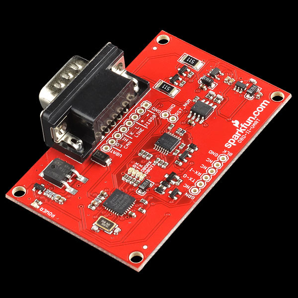
SparkFun's OBD-II interface board.

The OBD-II connector is always located in the passenger compartment, within three feet of the driver. Here is a database showing the approximate location for many makes and models. For my Escort and my wife’s Sable, the connector was found below the driver’s side dashboard, to the left of the steering wheel column.

Once the board is connected to the OBD-II connector and to the computer, a few commands are all that is needed to start reading data. Sending a query code of 010C returns the engine speed (in quarter-RPM, encoded in hex). Sending a query of 010D returns the current vehicle speed in km/hr (also encoded in hex).

Once you’re connected, the next step is learning the language. SparkFun provides a good bit of documentation and some examples on their site, and Wikipedia also has a nice list of many of the basic PIDs and what information they return.

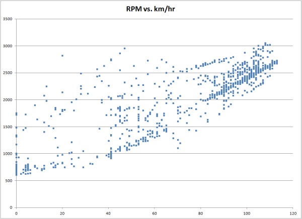
With a bit of programming, this information can be recorded, logged, and presented in nearly any format imaginable. Here, for example, is a plot of engine RPM vs. vehicle speed, for part of a recent trip I took.

A scatterplot of RPM vs. vehicle speed, for part of a trip. (Click for larger.)

The availability of the OBD-II bus not only allows the collection of data using a PC, but also provides a way to implement a custom vehicle computer system using an Arduino or similar microcontroller. (More about this, later!)



Posted in Arduino, Automotive, C, Coding, Digital, Electronics, HOW-TO | Tagged , , , , | Leave a comment

Mad Science : Jacob’s Ladder

I looked around the lab a few weeks ago and realized something was lacking. I mean, sure, I had some rubidium frequency standards, GPS puzzle boxes, and more PICs than I can shake a stick at, but something was missing — high voltage! (I mean, I do have one high-voltage DC supply, but that’s literally a Fluke.) A Jacob’s Ladder, or traveling-arc display, was clearly called for.

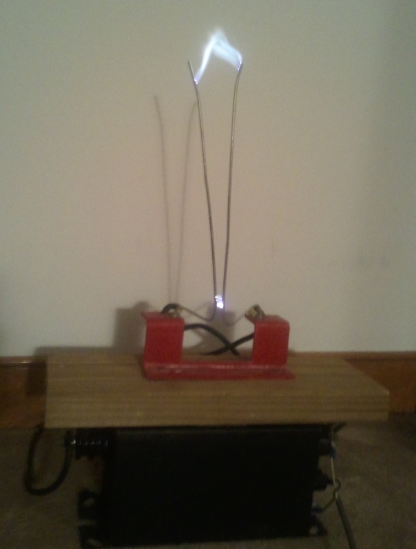
A high-voltage traveling-arc display, commonly known as a Jacob's Ladder. (Click for larger.)

DISCLAIMER: Traveling-arc displays require high voltage, which can injure or kill. The electrodes can get very hot when operating, and could poke you in the eye even when off, if you’re not careful. The transformer is also extremely heavy and could find all kinds of different ways to cause injury.
Don’t try this unless you know what you are doing!

Traveling-arc displays work by ionization of air. Two metal rods are installed in a shallow “V,” with a small gap at the bottom. When a high enough voltage is applied across the rods, the air gap at the base of the “V” breaks down. (The dielectric strength of air is about 3 million volts per meter, or roughly 1mm per kilovolt.) Once the air at the bottom of the V has been broken down and ionized, its conductivity increases quite a bit, allowing a significant current to flow. The air is heated by the power (V^2/R) dissipated in the arc, and begins to rise. Since this ionized air is the path of least resistance, the arc follows the rising air up the “V” until the arc either grows too long to be sustainable at the input voltage, or the top of the “V” is reached.

With sufficient voltage, the arc will remain at the top of the “V” indefinitely. What normally happens, though, is the arc breaks up when the air continues to rise. This raises the voltage between the rods, and the cycle begins again when the air at the bottom of the “V” breaks down once more and another arc rises.

A trip to eBay turned up a good deal on a used 9kV neon sign power supply. Carefully testing it out with a pair of paper clips proved the concept, so the next step was to build a larger “V.” Before I got around to that, though, I was lucky enough to find a 15kV Franceformer neon transformer at Slindy’s Flea Market (near Culpeper, VA). It even came with a bracket and metal “V” — someone else obviously had the same idea. (That’s it in the picture, above.)

A few adjustments to the electrodes later, it’s up and running, and would look right at home in Dr. Frankenstein’s lab. These things are best seen rather than described, though, so here’s a video.

Posted in DoNotTryThisAtHome, High Voltage, Mad Science, Science | Tagged , , | Leave a comment

Z80 delay loops

Since microprocessors typically run at clock speeds of several MHz, one important software task is to implement delays, to give peripherals (or users) time to respond to data.

There are several methods of producing delays, and each has advantages and disadvantages. One of the simplest methods is the spinloop — so named because the processor simply “spins” through the same small segment of code many times, taking up a given amount of time before continuing on to the next task.

With each instruction taking a fixed amount of time — and a limited number of memory locations available for instructions (65,536 on a 16-bit Z80; 256 on the 8-bit DrACo/Z80) — loops become necessary to implement all but the shortest delays. A counter (typically a register) is set to a certain value at the beginning of the loop, and is then decremented once on each pass through the loop. On each pass, the value in the register is checked to see if it is zero. If so, the processor breaks out of the loop and continues.

Even using 16-bit registers, though, only relatively short delays of perhaps a few hundred thousand clock cycles are possible (since the largest value that can be stored in 16 bits is 65,536.) To get longer delays, multiple loops are nested — one inside the other. This multiplies the loop delays: if both the inner and outer loops have a count of 1,000, the processor will execute the inner 1000-count loop 1000 times, resulting in a much longer delay (the inner loop goes through one million cycles total.)

By varying the values loaded into the registers, the length of the delay can be set to any reasonable value. If using a system clock of 1MHz, a delay of one million instructions would result in a one-second delay — suitable for blinking an LED. A delay of a thousand instructions would result in a one-millisecond delay — a useful interval between sending commands or data to a LCD display.

In Z80 assembly code, a nested delay loop would look something like this :

LD BC, 1000h            ;Loads BC with hex 1000
Outer:
LD DE, 1000h            ;Loads DE with hex 1000
Inner:
DEC DE                  ;Decrements DE
LD A, D                 ;Copies D into A
OR E                    ;Bitwise OR of E with A (now, A = D | E)
JP NZ, Inner            ;Jumps back to Inner: label if A is not zero
DEC BC                  ;Decrements BC
LD A, B                 ;Copies B into A
OR C                    ;Bitwise OR of C with A (now, A = B | C)
JP NZ, Outer            ;Jumps back to Outer: label if A is not zero
RET                     ;Return from call to this subroutine

This will produce a delay roughly proportional to BC * DE. Since both are 16-bit registers, you could set both to 0xFFFF, executing the inner loop up to some 4.2 billion times. Using lower numbers would reduce the delay — using 0x1000 for both as in the example above would be a delay of about 16 million inner loop executions. (The exact formula depends on the number of cycles needed for each instruction — but often, that kind of accuracy isn’t needed.)

The reason for the LD and OR commands is to logically OR the two halves of each 16-bit register together. (It turns out that when you increment or decrement 16-bit registers on the Z80, this doesn’t affect the zero flag, so the JP NZ would go on the information from the last 8-bit operation, which is not what we want. By comparing the two bytes of each register manually, the zero flag is set accordingly, and the JP NZ instruction works as expected.)


Posted in Assembly, Coding, Digital, DrACo/Z80, Drexel, EET325 | Leave a comment

Peripheral Interfacing on the 8-bit DrACo/Z80

The 8-bit breadboarded version of the DrACo/Z80 is a simplified version of the original 16-bit wire-wrapped computer from 2008. Switching to a simplified 8-bit design, along with switching to breadboard construction, allows the computer to be relatively easily completed and tested within a single ten-week term.

Interfacing with peripherals is still possible with the new design. Here is how I/O on Z80 computer systems works…

First, ~CE (Chip Enable) on the Cypress SRAM should be tied directly to the ~MREQ line on the Z80, instead of to Ground. This prevents the memory chip from responding when I/O requests (using the IN and OUT instructions) are used. This is the usual method of wiring ~MREQ. However, some recent versions of the 8-bit system were not intended for use with peripherals, so ~CE was simply tied to Ground on the Cypress chip. Fortunately, re-enabling peripheral compatibility is a one-wire fix.

Bus peripherals interface with the Z80 just like memory chips do: they should respond to reads (from the peripheral) when the ~IORQ and ~RD lines from the Z80 both go low, and they should respond to writes (to the peripheral) when the ~IORQ and ~WR lines from the Z80 both go low. (~RD and ~WR should never both be low at the same time.) Peripherals are also connected to the data bus (for reads and writes), and also read from the lower eight bits of the address bus (A0 through A7).

A typical read cycle (to read data in to the Z80 from a peripheral) would work like this:

  • The Z80 places the I/O address (00 through FF) on the lower 8 bits of the address bus.
  • The Z80 switches to input (read) mode on the data bus.
  • The Z80 lowers the ~IORQ and ~RD lines.
  • The Cypress memory chip sees the ~RD line low, but since the ~MREQ line is not also low, it ignores it and stays inactive.
  • Any peripherals on the bus see the ~RD line low and the ~IORQ line low. They then (using internal logic) compare the value of the address bus to their internal preset value. If it matches, they place their data (perhaps from a microphone or temperature sensor or voltage sensor etc) onto the data bus.
  • After a short delay, the Z80 reads the data from the data bus, and stores it in an accumulator (for an IN instruction) or prepares to send it back out to a memory location (for an INI instruction).
  • The Z80 then raises the ~IORQ and ~WR lines. This signals the peripheral that the write cycle is over (and that the peripheral needs to release the data bus now.)

Similarly, a write (to write data from the Z80 to the peripheral) works as follows:

  • The Z80 places the I/O address (00 through FF) on the lower 8 bits of the address bus.
  • The Z80 places the data to be written onto the data bus.
  • The Z80 lowers the ~IORQ and ~WR lines.
  • The Cypress memory chip sees the ~WR line low, but since the ~MREQ line is not also low, it ignores it and stays inactive.
  • Any peripherals on the bus see the ~WR line low and the ~IORQ line low. They then (using internal logic) compare the value of the address bus to their internal preset value. If it matches, they read the data from the data bus, and do whatever they do with it (output a sound, flash a light, change the state of a relay etc).
  • The Z80 then raises the ~IORQ and ~WR lines. This signals the peripheral that the write cycle is over.

If you know that you will only be using one I/O peripheral, you can skip the address-decoding part and simply trigger the peripheral to write to the bus when ~IORQ and ~RD are both low (remember, ~RD and ~WR are named from the Z80’s perspective), and read from the bus when ~IORQ and ~WR are both low.)

Posted in Assembly, Digital, DrACo/Z80, Drexel, EET325 | Leave a comment